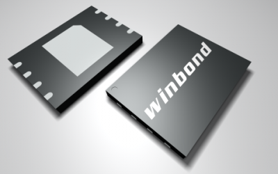
W25N01GVZEIG
1Gb Serial NAND Flash 104MHz SON8
Supplier:
Winbond
Certification:


Introduction:
The W25N01GV is a 1G-bit Serial SLC NAND Flash Memory developed by renowned manufacturer Winbond. This memory provides an excellent storage solution for systems with limited space, pins, and power, while also integrating the widely used SPI interface and massive non-volatile NAND memory space.
Function & Applications:
This memory device is a perfect fit for code shadowing to RAM, executing code directly from Dual/Quad SPI (XIP), and storing various forms of data such as voice, text, and more. It's particularly useful in applications necessitating efficient access to the entire memory array, thanks to its Continuous Read Mode.
With growing NAND flash densities, it has become an ideal solution for embedded designers aiming to store code on NOR flash systems beyond 512Mb. While NOR flash is cost-effective at lower densities, NAND flash like W25N01GV is preferred at 512Mb and above.
Performance Parameters:
The W25N01GV operates on a single 2.7V to 3.6V power supply, current consumption being as low as 25mA active and 10µA for standby. It can support SPI clock frequencies of up to 104MHz, allowing equivalent clock rates of 208MHz for Dual I/O and 416MHz for Quad I/O.
This memory offers a 50MB/S continuous data transfer rate and demonstrates a page read time with ECC Enable of 50us, and page program time of approximately 250us. Additionally, it has a block erase time of 2ms(typ.)
Package Types, Interface & Pin Configuration:
The W25N01GV supports standard Serial Peripheral Interface (SPI), Dual/Quad I/O SPI including different data I/O. It is available in various space-saving packages including 8-pad WSON 8x6-mm, 16-pin SOIC 300-mil, and 24-ball TFBGA 8x6-mm.
Reliability & Lifespan:
The product promises exceptional reliability with 100,000 erase/program cycles and 10-year data retention. To provide better NAND flash memory manageability, user-configurable internal ECC, and bad block management are also available in W25N01GV.
Standards & Certifications:
The device meets industry standards and supports JEDEC standard manufacturer and device ID. Furthermore, it includes features like Unique ID page, Parameter page, and ten 2,048-Byte OTP pages.
Application Cases & Reference Designs:
The W25N01GV is effective in a range of applications, offering not just normal data storage but also efficient code shadowing and directly executing code from Dual/Quad SPI (XIP). With its built-in ECC and bad block management, it offloads day-to-day functionalities from the controller, simplifying the process for embedded designers and programmers. Furthermore, its unique "continuous read" functionality proves beneficial for swift content transfer from NAND to DRAM.
Product Feature 1
Page Program Time: 250us(typ.)
Block Erase Time: 2ms(typ.)
Support OTP Memory Area
Datasheet
Datasheet


