APPLICATION NOTE

The Next Innovation in High Density and Low Pin Count

SpiStack® is Winbond’s new W25M series developed to meet the demand for higher density, while maintaining
a low pin count of the SpiFlash® packages. This innovation brought about the advantages of concurrent operations,
i.e., Read while Program or Erase functions and added combination of two technologies, NOR and NAND flash
memories.
Key features
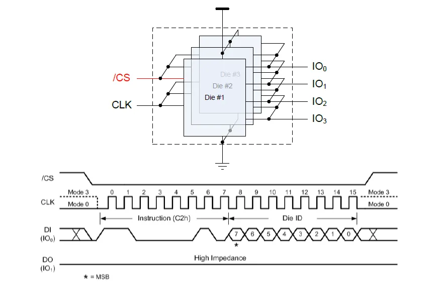
The SpiStack® Die Selectability. The Chip Select signal is ganged across all dies. Each die has its own unique
factory programmed 8-bit Die ID. A Software Die Select command code, C2h followed by the 8-bit die address
0x00 thru 0x03, in the case of a four die stack configuration. Die 0x00 is always active after power-up or after a
Reset command. The Software Die Select command can be issued at any time regardless of its operating state to
select another die in the stack.
A performance benefit feature of the SpiStack® is Concurrent Operations, which allows reading the contents of
one die while programing or erasing another. In the case of three or more die, Multi-Die Program/Erase while Read
is possible.
The SpiStack® allows for Homogenous or Heterogeneous Multiple Chip Packages (MCP) configurations.
Homogeneous configurations, stack identical densities either in stack dies of SpiFlash® NOR or stack dies of
SpiFlash® NAND. Heterogeneous SpiStack® , combines the two technologies of NOR and NAND, that consist of
a smaller density and high reliability Code Storage NOR and a higher density, faster program and erase speeds Data
Storage NAND.
Software Die Selection (C2h)
The Software Dies Select is used to select any die within the Multiple Chip Package (MCP). The 8-bit command
C2h, followed by the 8-bit die address can be issued at any time to activate another die, deactivating the current die
regardless of their operating state allowing the single Chip Select (/CS) to be recognized by the active die.

Figure 1: Die Selectability
Concurrent Operations
Typical SpiFlash® operates in a sequential pattern of commands, addresses and data. Where Read operations will
have control of the SPI Bus and Program or Erase functions leave the SPI bus idle while the time is spent executing
the operation.
In the case of a SpiStack® MCP, Concurrent Operations can be realized by assigning the current Active Die to
perform an Erase/Program operation which requires some amount of time to finish. While the internal
Program/Erase operation is on-going, the controller can issue a “Software Die Select (C2h)” instruction to select
another die to be active. Depending on the system requirement, a Read, Program or Erase operation can be
performed on the newly selected Active Die. “Read while Program/Erase” or “Multi-Die Program/Erase” can be
performed in such fashion, to improve system Program/Erase throughput and to avoid constant Program/Erase
Suspend and Resume activities in certain applications.
Sequential Operations

Concurrent Operations

Figure 2: SpiStack® Concurrent Operations vs Conventional SpiFlash® Operations
Homogenous and Heterogeneous Configurations
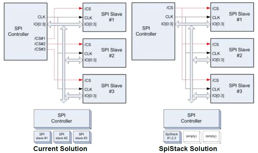
SpiStack® allows the choice of two types of configurations, Homogenous and Heterogeneous where small pin
count, small form factors and flexible combination of densities and flash technologies are certainly possible.
Homogeneous SpiStack® , stacks either the same SpiFlash® (NOR + NOR) or Serial SLC NAND Flash (NAND
+ NAND) die densities in a convenient low pin-count packages while significantly increasing the memory density
by a factor of the number die contained in the specified package. Sometimes the increase in density is proportional
to the increase in die size that just fits in a particular package, but with the SpiStack® you can double or even
quadruple the density with only the package height being the limiting factor.
Heterogeneous SpiStack® , stacks the serial NOR and SLC NAND flash technologies of different densities in the
same MCP package. This allows for the choice of code storage from the SpiFlash® memory dies of a smaller
density to be combined with the high performance and high density data storage from the Serial SLC NAND Flash
dies all sharing the same SPI Bus.

Figure 3: SpiStack® Comparison
Drivers and Simulation Models
Drivers and Simulation Models can be obtained by contacting the Winbond Electronic Corporation of America
Technical Support. (Click Here)
Revision History

Trademarks
Winbond, SpiFlash and SpiStack are trademarks of Winbond Electronics Corporation.
All other marks are the property of their respective owner.
Important Notice
Winbond products are not designed, intended, authorized or warranted for use as components in systems or equipment
intended for surgical implantation, atomic energy control instruments, airplane or spaceship instruments, transportation
instruments, traffic signal instruments, combustion control instruments, or for other applications intended to support or
sustain life. Furthermore, Winbond products are not intended for applications wherein failure of Winbond products could
result or lead to a situation wherein personal injury, death or severe property or environmental damage could occur.
Winbond customers using or selling these products for use in such applications do so at their own risk and agree to
fully indemnify Winbond for any damages resulting from such improper use or sales.
Information in this document is provided solely in connection with Winbond products. Winbond reserves
the right to make changes, corrections, modifications or improvements to this document and the products
and services described herein at any time, without notice.
AN0000011
Publication Date: April 06, 2017 Revision 1.0


