
APPLICATION NOTE

Serial Flash PCB Layout GuidelinesSerial Flash PCB Layout Guidelines

Introduction
This document provides information on Winbond’s SpiFlash® NOR memory packages and suggested PCB land patterns.
Content
The following sections contain detailed Package Outline Drawings with mechanical descriptions of Winbond’s SpiFlash® packages and the related suggested PCB land patterns.
There are three main section SOP, SON and TFBGA.
SOP Packages; SOP8 150 MIL, VSOP8 150 MIL, SOP8 208 MIL, VSOP8 208 MIL, and SOP16 300 MIL
SON Packages; USON8 3x2mm, USON8 3x4mm, USON8 4x4mm, WSON8 6x5mm, and WSON8 8x6mm
BGA Packages; TFBGA24 6x8mm 4x6 matrix and TFBGA24 6x8mm 5x5 matrix
SOP Packages
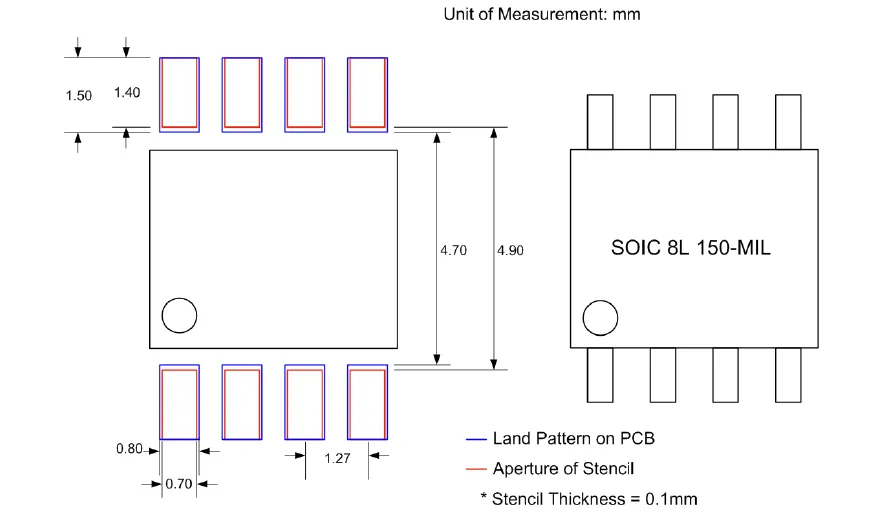
SOP8 150 MIL
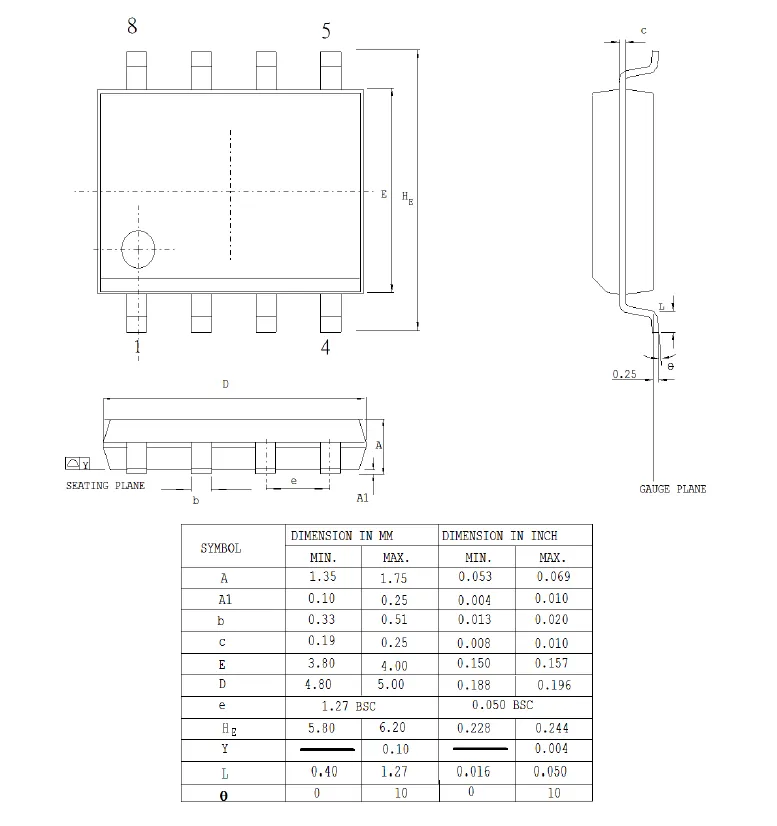
8L SOP 150-MIL Land Pattern
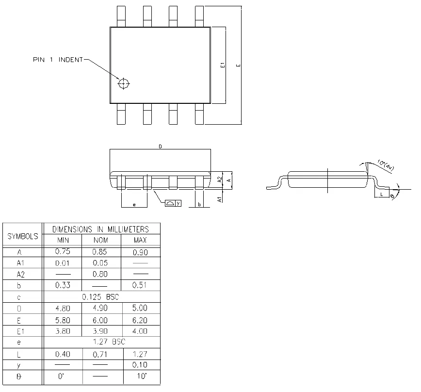
VSOP8 150 MIL
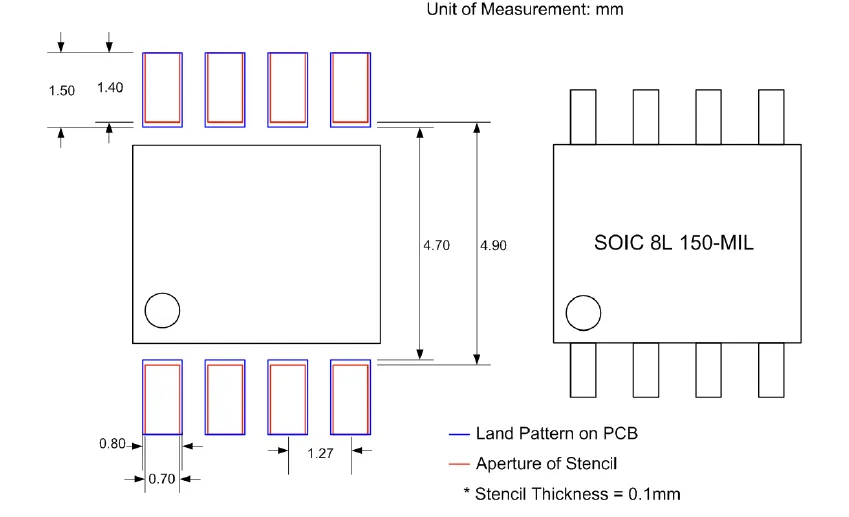
8L SOP 150-MIL Land Pattern
SOP8 208 MIL
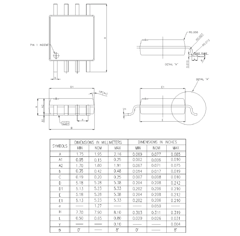
8L SOP 208-MIL Land Pattern
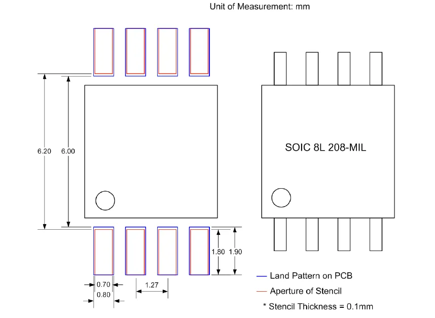
VSOP8 208 MIL
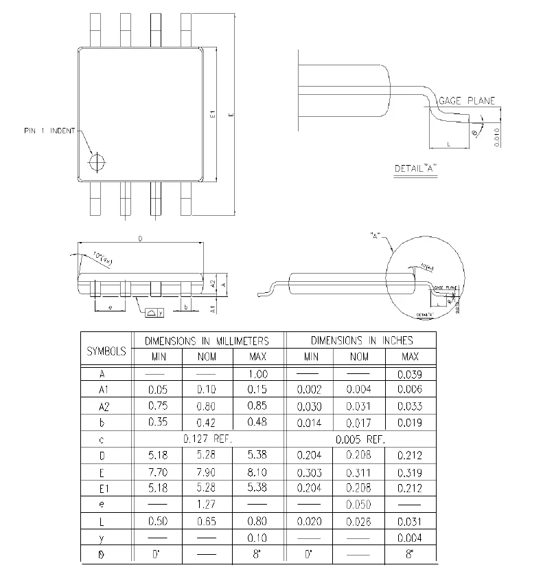
8L SOP 208-MIL Land Pattern
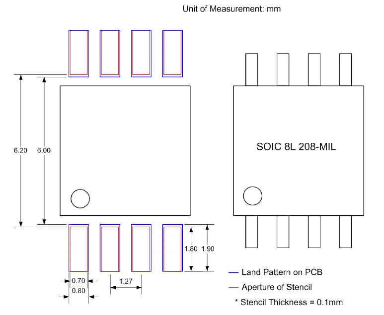
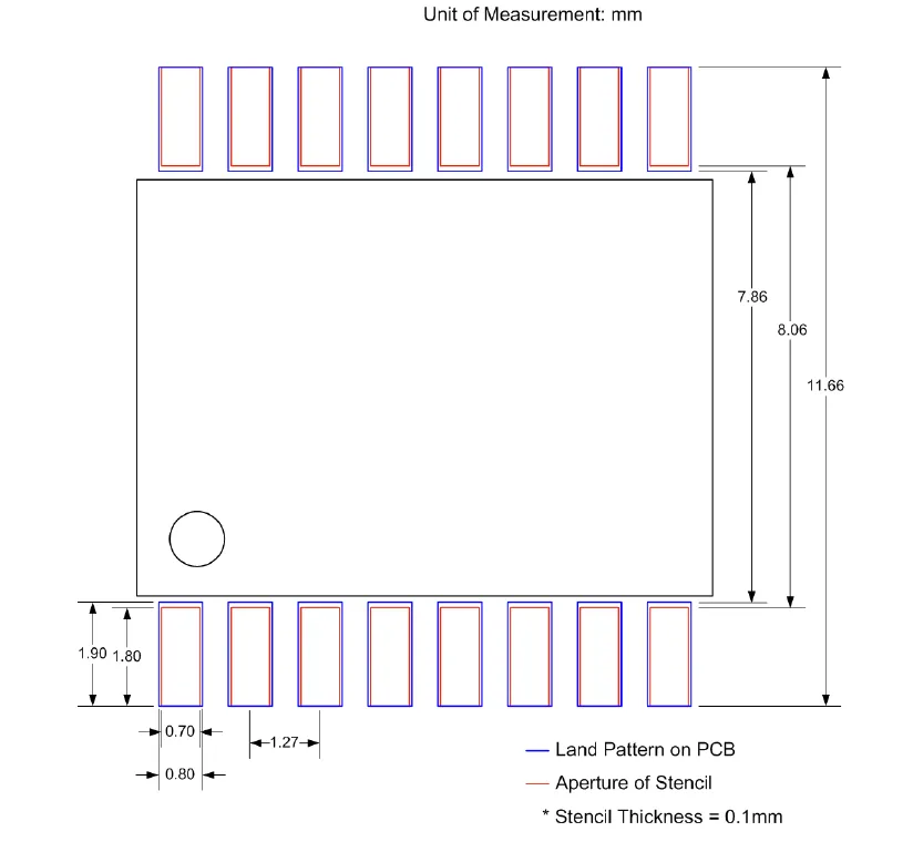
SOP16 300 MIL
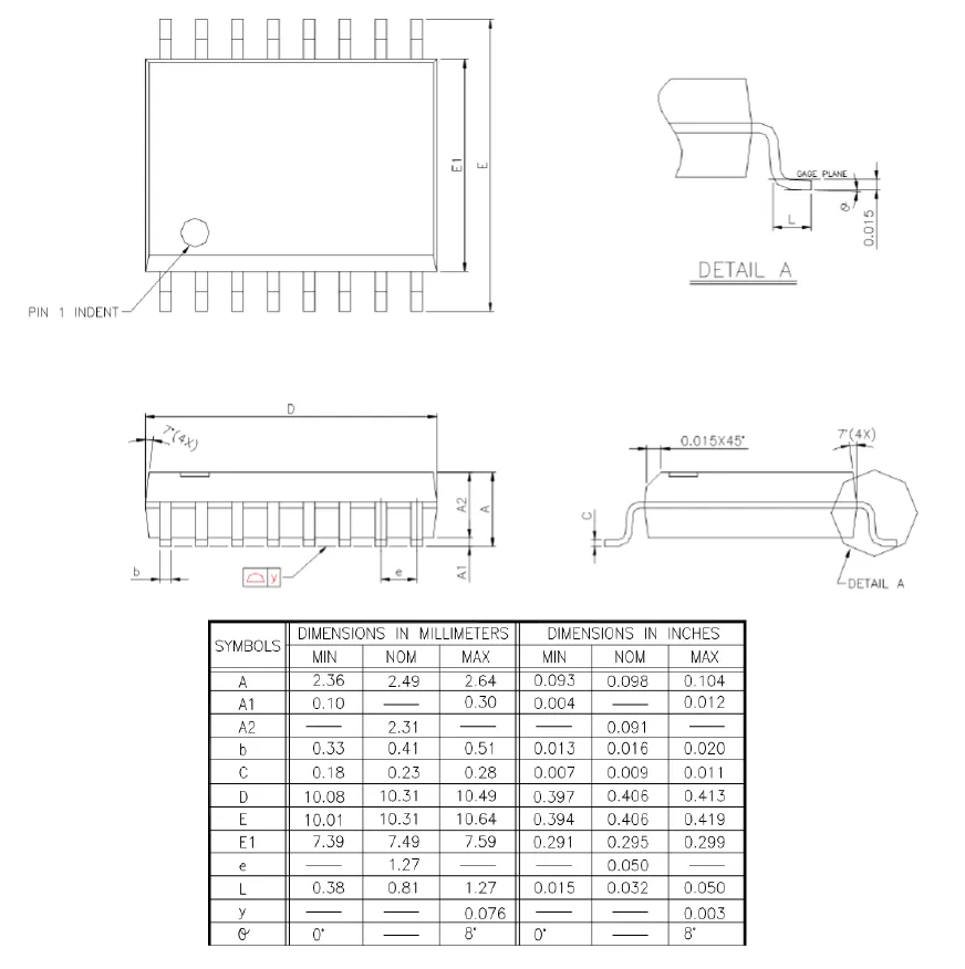
16L SOP 300-MIL Land Pattern
SON Packages
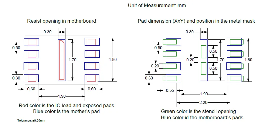
USON8 3x2mm
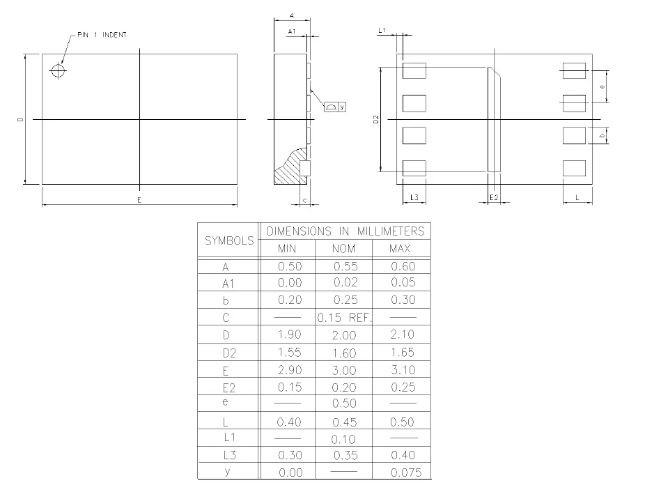
USON8 3x2MM Land Pattern
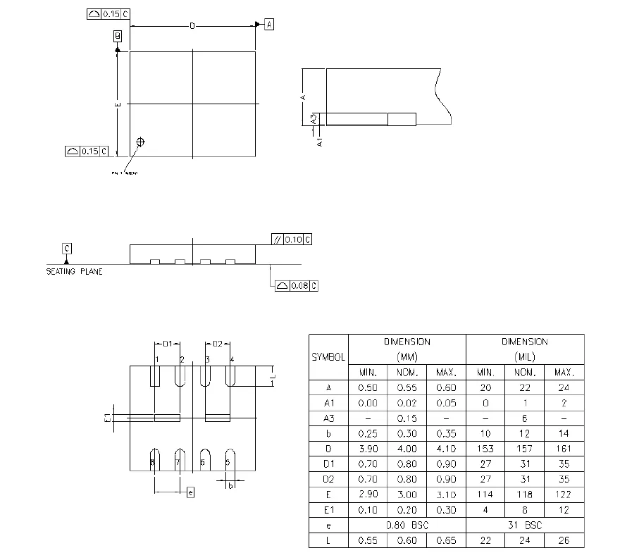
USON8 3x4mm
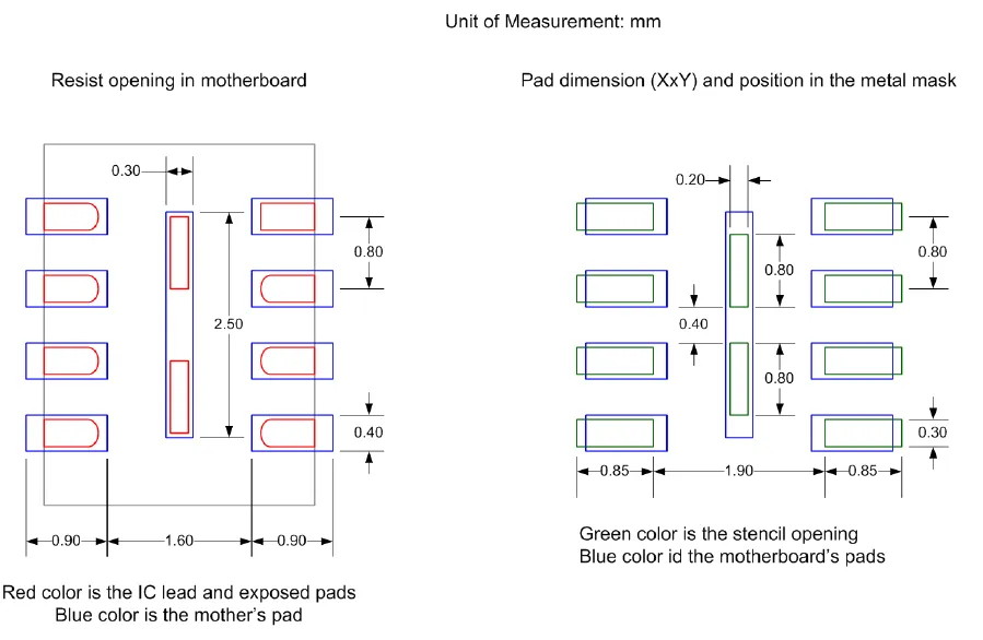
USON8 4X3MM Land Pattern
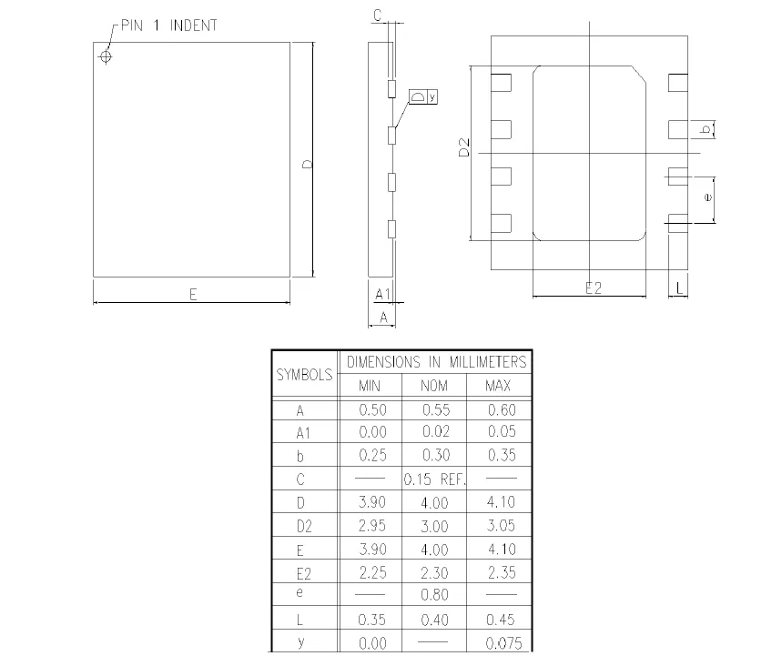
USON8 4x4mm
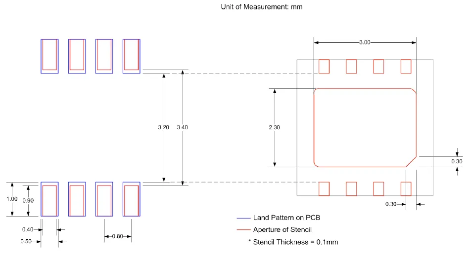
USON8 4x4mm Land Pattern
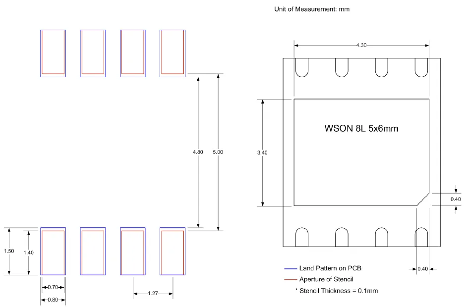
WSON8 6x5mm
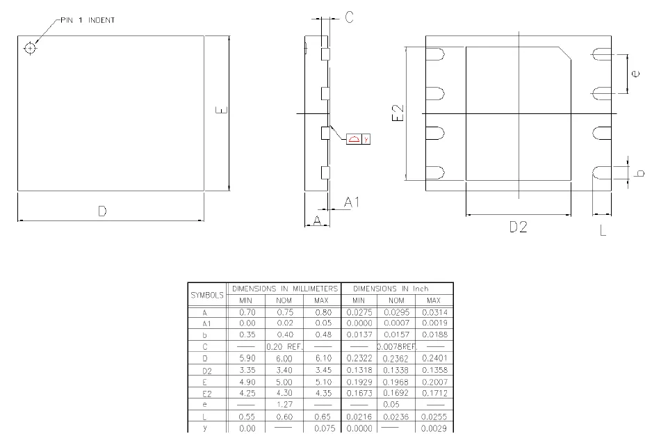
WSON 8L 5x6mm Land Pattern
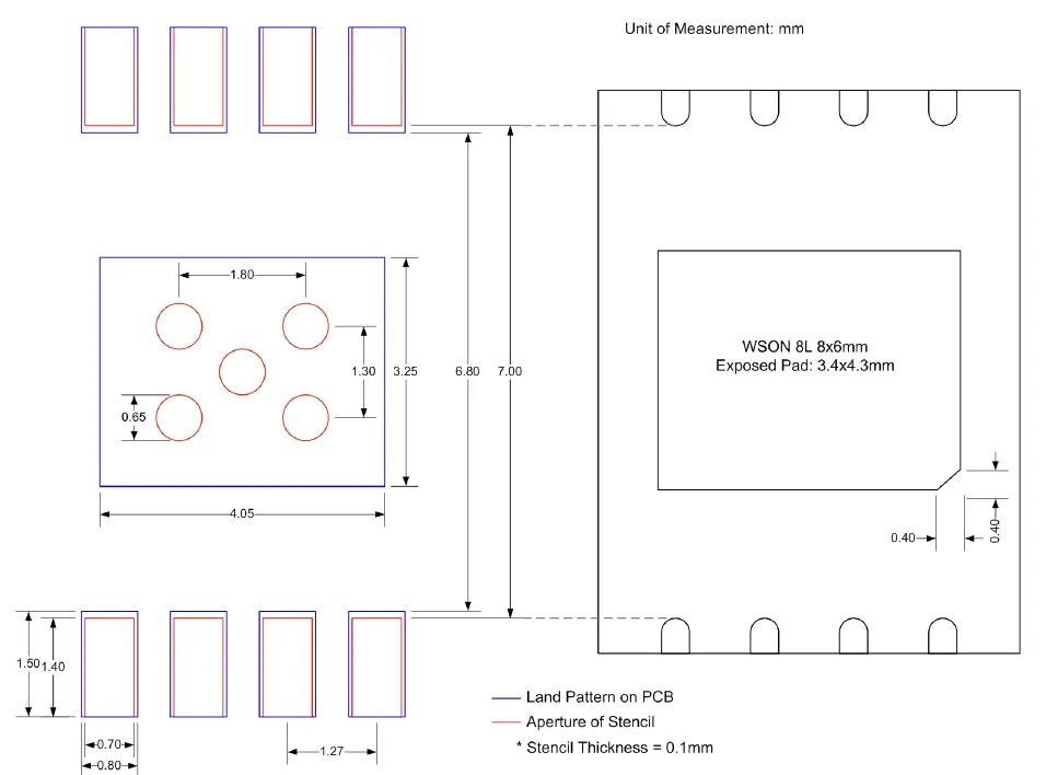
WSON8 8x6mm
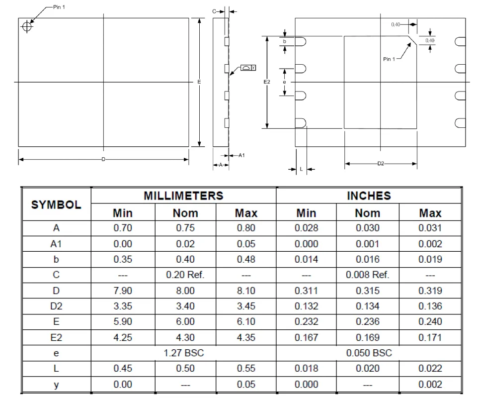
WSON 8L 8x6mm Land Pattern
BGA Packages
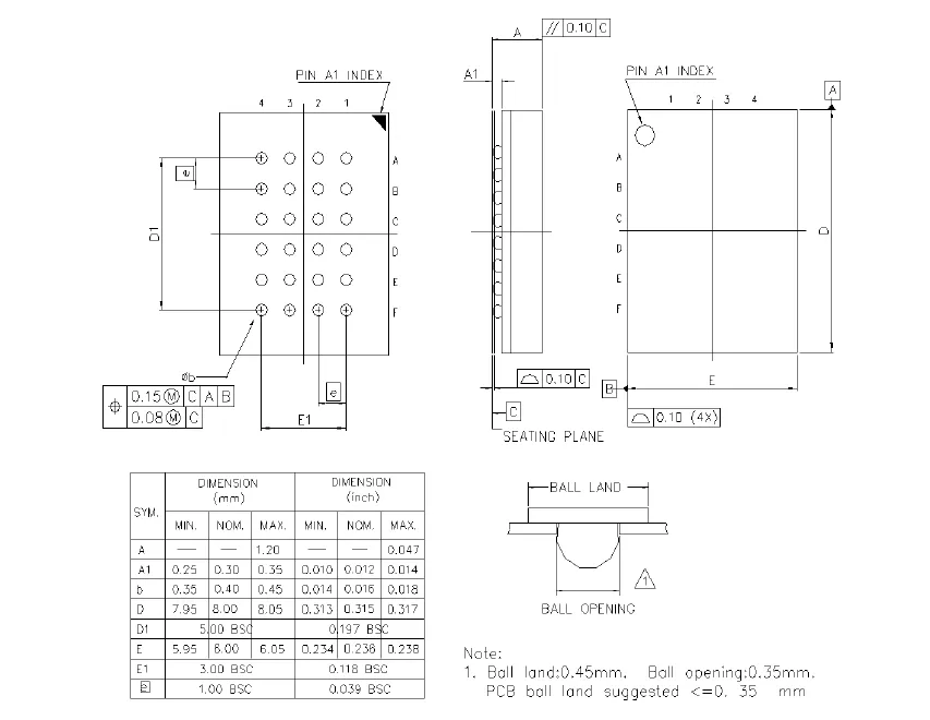
TFBGA24 6x8mm 4x6 matrix
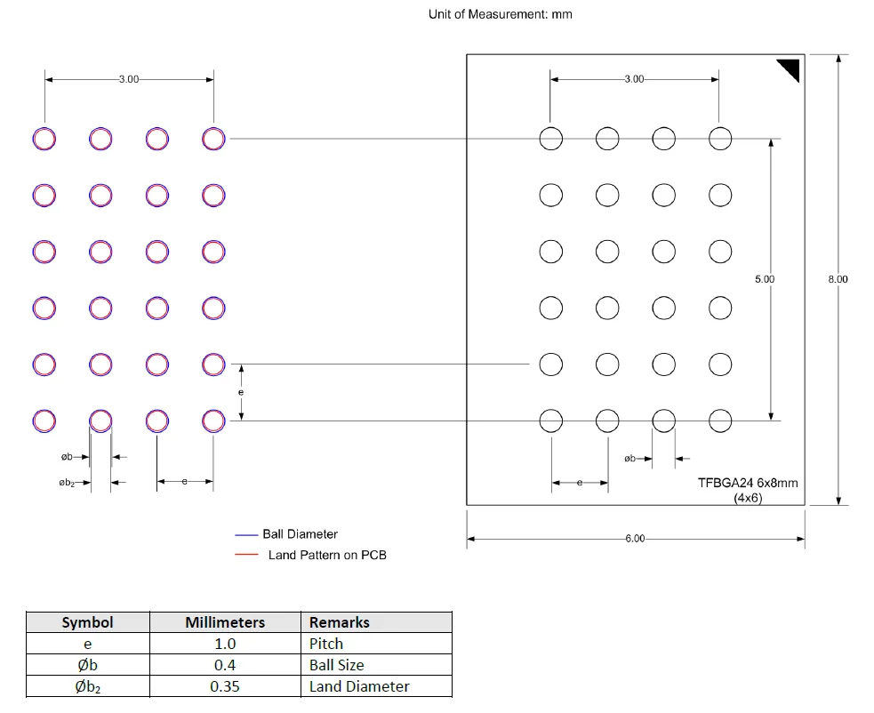
TFBGA24 6x8mm 4x6 matrix Land Pattern
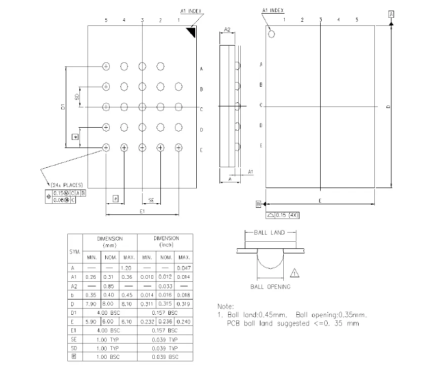
TFBGA24 6x8mm 5x5 matrix
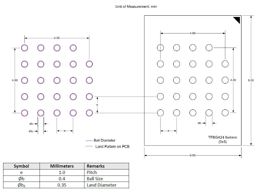
TFBGA24 6x8mm 5x5 matrix Land Pattern
Revision History

Trademarks
Winbond, SpiFlash and SpiStack are trademarks of Winbond Electronics Corporation.
All other marks are the property of their respective owner.
Important Notice
Winbond products are not designed, intended, authorized or warranted for use as components in systems or equipment intended for surgical implantation, atomic energy control instruments, airplane or spaceship instruments, transportation instruments, traffic signal instruments, combustion control instruments, or for other applications intended to support or sustain life. Furthermore, Winbond products are not intended for applications wherein failure of Winbond products could result or lead to a situation wherein personal injury, death or severe property or environmental damage could occur. Winbond customers using or selling these products for use in such applications do so at their own risk and agree to fully indemnify Winbond for any damages resulting from such improper use or sales.
Information in this document is provided solely in connection with Winbond products. Winbond reserves the right to make changes, corrections, modifications or improvements to this document and the products and services described herein at any time, without notice.
AN0000009
Publication Date: June 12, 2020 Revision 2.1


